- Nameadmin
- Date2016/04/11 00:00
- Hit487
- Realized all process of electronic element manufacturing by low-cost solution process for the first time in the world
- Key source technology of nano field that is immediately applicable to the high-tech industry such as flexible display
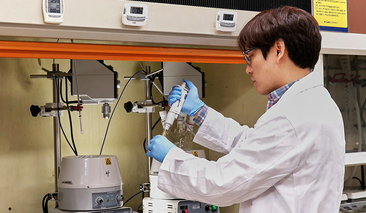
A study that realized all elements of electronic element (Thin Film Transistor, TFT)*, the core of high-tech electronic industry such as flexible display, as inorganic nanoparticles*** that enable solution process** was presented by a domestic researcher for the first time in the world.
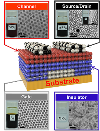
* Thin Film Transistor (TFT) is an element controlling the basic drive of pixel, which is the minimum image unit of LCD and OLED. It consists of several thin films and is composed of three metal electrodes—gate, source, and drain—, insulation layer, and semiconductor layer which is the path that electricity flows through.
** Solution process is a method of liquefying materials using organic solvent and metallizing them on a board through spin-coating, ink-jet printing, etc. Vacuum evaporation is a method of making thin films on the surface of board that is facing the evaporation source by evaporating metal or compounds from vacuum. The solution process has a lower facility investment cost compared to the vacuum evaporation method and enables a faster process with small-scale equipment. It recently has received the attention of electronic industry as a new method to lower the price of OLED panel.
*** Nanoparticle is a particle less than the size of 100nm (nanometer=1m over 10 billion). There are countless ways of applying nanoparticles usefully depending on their size, structure, and how they are arranged, combined, and mixed. Especially, semiconductor nanoparticle, also called as Quantum dot, is used widely in ultra-high definition TV, etc. as its electrical and optical characteristics can be controlled by adjusting its size.
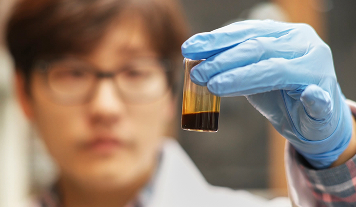
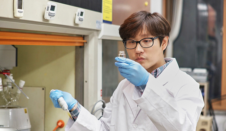
The research results of realizing high functional inorganic nanoparticle thin film that was performed by Dr. Jihyeok Choi in the Rare Resource Use Research Lab of Mineral Resource Research Center in the Korea Institute of Geoscience and Mineral Resources (Director Kyuhan Kim, KIGAM) was published on Science, a top 3 science journal in the world. KIGAM is a government-funded research institute by the Ministry of Science, ICT and Future Planning.
Dr. Choi participated as the lead author in a research paper on the ‘Organic Combination System of Inorganic Nanoparticles to Realize High Functional (Exploiting the Colloidal Nanocrystal Library to Construct Electronic Devices)’, which was published in Science on April 8th. Also, Professor Cherie R. Kagan in the University of Pennsylvania, Dr. Choi’s advisory professor, was put on the paper as the contact author. Co-authors included Professor Christopher Murray in the University of Pennsylvania, Professor Seungjoo Oh in Korea University, Dr. Jinwoo Seong in Yonsei University, and the research team in the University of Pennsylvania.
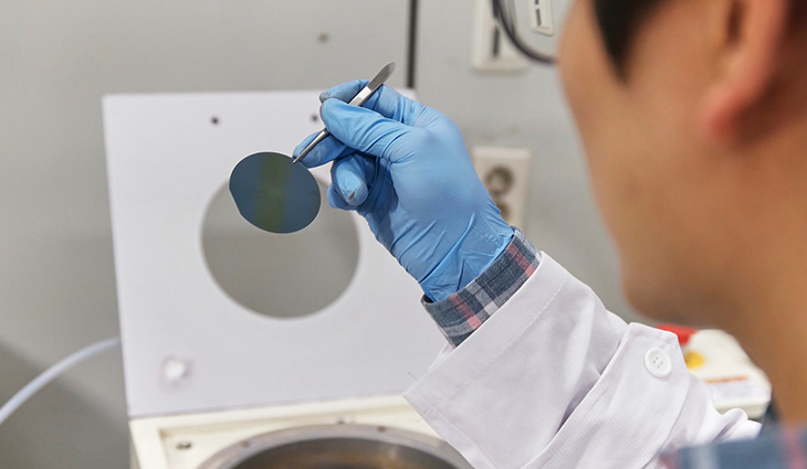
Recently, nanoparticles are made in the form of thin film that can be used easily and is examined as a core material of high functional next generation. The inorganic nanoparticles of thin film can be produced in large quantity at low cost through the solution process and can be easily applied to a wide surface area. Thus, it is highly favored as a next generation electronic component material that will replace the silicon-based semiconductor industry of the existing vacuum evaporation method.
However, one disadvantage of making inorganic nanoparticles in a thin film is that it has a noticeably low electrical conductivity. This is because of organic elements that exist in between nanoparticles when they are mixed and combined in a thin film form.
Therefore, the application of nanoparticle thin film has remained at an experimental level so far. Such use has been limited to as one component part within an electronic element; the other parts of the element need enormous equipment and have been made through the existing, traditional vacuum evaporation process that has a huge cost burden.
However, the above problem can be solved through a simple solution process by using Dr. Choi’s study results published on the Science paper. By applying the new technology proposed by Dr. Choi, all component parts of electronic element (thin film transistor, TFT) can be made based on the low cost solution process instead of the traditional vacuum evaporation method. A source technology to optimize the combination system of nanoparticle thin film has been secured for the first time in the world.
While nanoparticle thin film was made and used based on the solution process before, it was limited to making partial elements as its reliability could not be secured. However, Dr. Choi successfully secured a technology that will not decrease the functions of nanoparticles in the thin film making through the solution process and in the lamination of the multiple layers of nanoparticle thin films. He also succeeded in applying the solution process to all elements.
Especially, doping process is done to activate the semiconductor layer in the last stage of electronic element making, and even this doping process that used to apply the vacuum evaporation can be done by the solution process. This means that Dr. Choi’s work is the first research that achieved the true ‘Processing of All Process Solution (All Solution, All Inorganic Nanocrystal-based).’
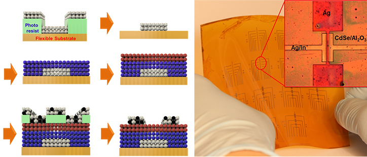
In addition, another advantage of solution process that will replace the vacuum evaporation process is that it is a low temperature process that can be handled on the plastic board. Considering this, there is infinite potential of this technology that can handle all process up to the doping stage by the solution process. One reason that glass board could not be replaced by a flexible plastic board is due to the fact that transparent plastic has ended up melting by high temperature vacuum evaporation.
For this research, Dr. Choi developed various nanotechnologies that enable solution process, and realized a high functional nanoparticle thin film that meets the characteristics of thin film in vacuum evaporation by effectively converging each technology. To make a high functional nanoparticle thin film, the distances among nanoparticles must be reduced, and electronic coherence among them must be enhanced. Especially, the flaws of nanoparticle surface must be controlled, and necessary electric charge must be inserted effectively to nanoparticles.
This research means the securing of source technology that can optimize the combination system of nanoparticle thin film that has the characteristics of conductor, semiconductor, and insulator. It is expected that all component parts of the existing electronic elements can be replaced based on the low-cost solution process.
Especially, this technology is highly likely to be commercialized as it can be immediately applied to the mass production of optimized semiconductor, which is currently used by the electronic industry. Also, since this technology that uses the solution process has a low facility expense and can realize by small-scale equipment, it can open a path for small and medium-sized companies that relatively lack funds to enter the electronic element manufacturing industry.
Lead author Dr. Jihyeok Choi in the Korea Institute of Geoscience and Mineral Resources said, “Nano research will take a step further from a basic field and become more active as a practical research to be applied to all electronic parts for everyday use. Depending on the demand of industry, it will be applied to various fields.”
Dr. Jihyeok Choi (35) is a rising scientist who is gaining worldwide recognition in the research of nano-material synthesis and characteristic evaluation. He graduated from the Department of Metal Engineering in Yonsei University and obtained a Ph.D. in the same institution. After the doctorate, he completed a training course in the University of Pennsylvania and was hired by the Korea Institute of Geoscience and Mineral Resources through the overseas public employment in 2014 and now works as a senior researcher at the Rare Resource Use Research Lab in the Korea Institute of Geoscience and Mineral Resources. He is currently performing a research to make graphene and graphene- nanoparticle composite that are high value added nanomaterials from natural minerals.
Director Kyuhan Kim in the Korea Institute of Geoscience and Mineral Resources said, “This research is an outstanding achievement that can further strengthen the technology of Korean industry that is leading electronic products and the semiconductor field. We will generously support a creative research environment so that researchers like Dr. Choi can take bigger parts on international stage.”